Introduction
Printed Circuit Board Assembly (PCBA) is a critical step in the manufacturing of electronic devices. It involves the mounting of electronic components onto a printed circuit board (PCB) to create a fully functional electronic assembly. This process is crucial for industries such as medical devices, aerospace, industrial automation, and consumer electronics. In this comprehensive guide, we will explore the various aspects of PCBA, including its importance, processes, technologies, and best practices.
What is Printed Circuit Board Assembly (PCBA)?
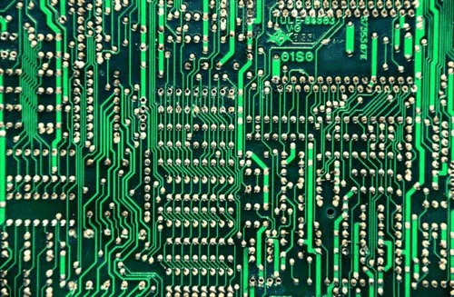
PCBA refers to the process of soldering or assembling electronic components such as resistors, capacitors, integrated circuits, and connectors onto a PCB. The assembly process transforms a bare PCB into a working electronic circuit capable of performing the intended functions.
Importance of PCBA
- Functional Integration: PCBA allows the integration of complex electronic components into a single compact unit.
- Reliability: High-quality assembly ensures the reliability and longevity of electronic devices.
- Scalability: PCBA enables mass production of electronic products with consistent quality.
- Customization: Advanced PCBA techniques allow for the development of customized electronic solutions tailored to specific applications.
Key Components of a PCB Assembly
- Bare PCB: The foundational structure that provides the physical and electrical base for component placement.
- Surface-Mount Devices (SMDs): Components mounted directly onto the PCB surface.
- Through-Hole Components: Components with leads that pass through holes in the PCB and are soldered on the opposite side.
- Solder Paste: A mixture of flux and solder powder applied to PCB pads for soldering surface-mount components.
- Pick-and-Place Machines: Automated equipment used to position components accurately on the PCB.
- Reflow Oven: Used to heat the assembly and solder the components in place.
- Inspection and Testing Equipment: Tools such as Automated Optical Inspection (AOI) and X-ray inspection to verify assembly quality.
PCBA Processes
1. Design for Manufacturing (DFM) Review
Before assembly, the PCB design undergoes a DFM review to ensure manufacturability, focusing on aspects such as:
- Component placement
- Soldering feasibility
- Thermal management
- Signal integrity
2. Solder Paste Application
Solder paste is applied to the PCB pads using a stencil printing process to ensure precise deposition.
3. Component Placement
Automated pick-and-place machines position components onto the solder-pasted board with high precision.
4. Reflow Soldering
The assembled board is passed through a reflow oven where controlled heating melts the solder paste, creating secure electrical connections.
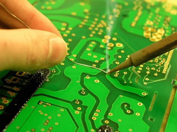
5. Through-Hole Component Insertion (if applicable)
For mixed-technology PCBs, through-hole components are inserted manually or via automated insertion machines.
6. Wave Soldering
For through-hole components, wave soldering involves passing the board over a wave of molten solder to form strong joints.
7. Inspection and Quality Control
Inspection techniques include:
- Automated Optical Inspection (AOI)
- X-ray inspection for BGA components
- Functional testing to verify performance
8. Final Assembly and Packaging
Once the PCB passes all quality checks, it is assembled into the final product housing and packaged for distribution.
Advanced PCBA Technologies
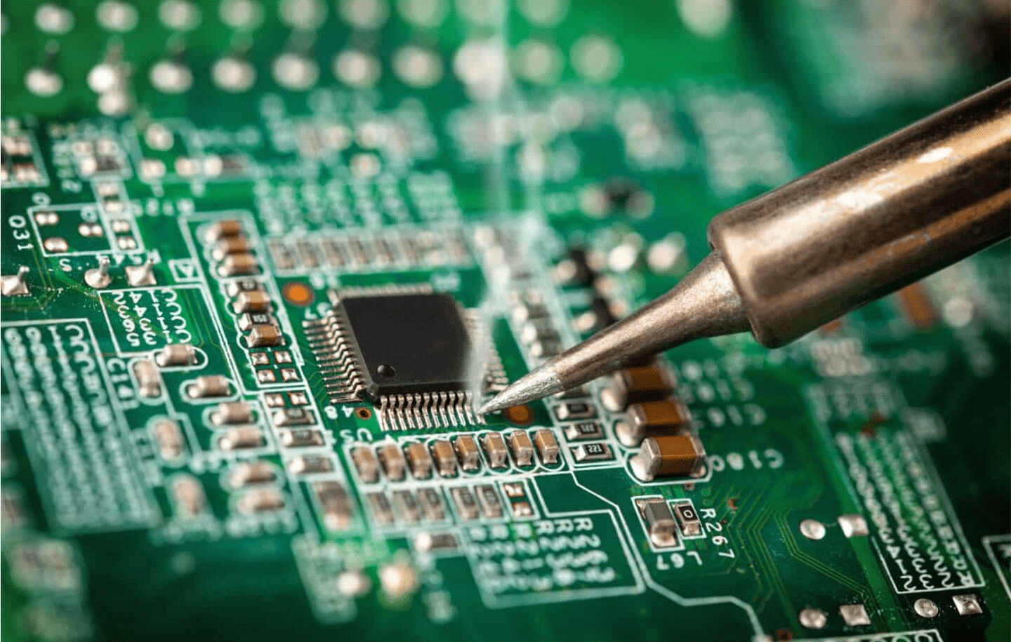
1. Surface Mount Technology (SMT)
SMT allows for smaller, lighter, and more complex designs by mounting components directly onto the PCB surface.
Advantages:
- Higher component density
- Faster production
- Reduced material costs
2. Through-Hole Technology (THT)
THT provides strong mechanical bonds, making it suitable for high-reliability applications.
Advantages:
- Enhanced durability
- Better thermal dissipation
- Easier manual rework
3. Mixed Technology Assembly
Combining SMT and THT techniques allows for hybrid PCB designs, catering to diverse functional and mechanical requirements.
4. Flexible and Rigid-Flex PCBs
Flexible and rigid-flex PCBs enable designs that can bend and conform to specific shapes, ideal for wearable electronics and aerospace applications.
5. High-Density Interconnect (HDI) Technology
HDI PCBs feature finer traces, smaller vias, and higher layer counts, enabling miniaturization and improved performance.
Quality Standards and Certifications in PCBA
Ensuring the highest quality in PCBA is crucial, especially in regulated industries like medical and aerospace. Key certifications include:
- ISO 9001:2015: Quality management system ensuring consistent performance.
- AS9100D: Aerospace industry-specific quality standards.
- ISO 13485:2016: Medical device quality standards.
- IPC-A-610: Acceptability standards for electronic assemblies.
- RoHS Compliance: Ensuring environmentally friendly manufacturing by restricting hazardous substances.
Common Challenges in PCBA and Solutions
1. Component Shortages
Solution: Partnering with reliable suppliers and leveraging alternative component sourcing strategies.
2. Soldering Defects
Solution: Optimizing reflow profiles, stencil design, and ensuring proper handling of components and solder paste.
3. PCB Warpage
Solution: Using appropriate board thickness and layer stack-up strategies.
4. Electromagnetic Interference (EMI)
Solution: Proper grounding, shielding, and layout techniques.
5. Thermal Management
Solution: Utilizing heat sinks, thermal vias, and strategic component placement
Conclusion
Printed Circuit Board Assembly (PCBA) is a cornerstone of modern electronics manufacturing. From initial design to final product assembly, each step in the process plays a crucial role in ensuring performance, reliability, and scalability. By adhering to best practices and leveraging advanced technologies, manufacturers can deliver high-quality electronic products that meet industry standards and customer expectations.
Contact us today to learn how our PCBA solutions can bring your product vision to life. Visit VergentProducts.com for more information.
Frequently Asked Questions (FAQs) about Printed Circuit Board Assembly (PCBA)
2. What are the key steps in the PCB assembly process?
The PCB assembly process includes the following steps:
- Design for Manufacturing (DFM) Review: Ensuring manufacturability and compliance with IPC standards.
- Solder Paste Application: Applying paste onto board pads using stencils.
- Component Placement: Automated pick-and-place of surface-mounted and through-hole components.
- Soldering: Using reflow or wave soldering techniques.
- Inspection: Quality control through automated optical inspection (AOI), X-ray inspection, and functional testing.
- Final Assembly and Packaging: Preparing the assembled boards for delivery.
3. What are the different types of PCB assembly technologies?
PCB assembly can be categorized into:
- Surface Mount Technology (SMT): Components are placed directly onto the PCB surface.
- Through-Hole Technology (THT): Components are inserted into holes drilled through the PCB.
- Mixed Technology Assembly: Combining SMT and THT for complex designs.
Rigid and Flex PCBs: Offering solutions for both flexible and rigid circuit board designs.
4. What factors should be considered when designing a PCB?
When designing a printed circuit board, key factors to consider include:
- Layer stack-up design for signal integrity and thermal management.
- Component placement and trace routing.
- Design for testability (DFT) to facilitate easier inspection and testing.
- Compliance with industry standards like IPC-A-610.
- Use of quality components and proper board assembly techniques.
5. What are the quality control measures in PCB assembly?
Quality control in PCB assembly involves:
- Automated Optical Inspection (AOI): Identifies assembly defects.
- X-ray Inspection: Examines hidden solder joints.
- Functional Testing: Ensures the board meets required operational parameters.
- Manual Inspection: Reviewing boards for any remaining issues.
Compliance with Industry Certifications: Such as ISO 9001, AS9100, and IPC standards.
6. What are the most common PCB assembly defects and how can they be prevented?
Common PCB assembly defects include:
- Solder Bridges: Prevented by using accurate solder paste application and stencils.
- Cold Solder Joints: Avoided through proper reflow profiles.
- Component Misalignment: Ensured with precise pick-and-place machines.
- PCB Warpage: Managed with appropriate materials and layer stack-up strategies.
Electromagnetic Interference (EMI): Minimized by correct grounding and shielding.
7. How do I choose the right PCB assembly company?
When selecting a printed circuit board assembly company, consider:
- Their experience in electronics manufacturing and industry-specific requirements.
- Certifications such as ISO 13485 (medical devices) and AS9100 (aerospace).
- The range of services offered, including prototyping and high-volume manufacturing.
- Quality control processes and adherence to IPC standards.
- Cost estimation tools like an online PCB assembly calculator.
8. What materials are used in PCB fabrication?
Printed circuit boards are typically made from:
- FR4: A common fiberglass-reinforced material.
- Metal-Core PCBs: Used for heat dissipation in power electronics.
- Flex and Rigid-Flex Materials: For applications requiring flexibility.
- Copper Traces: Providing electrical conductivity.
Solder Paste: For component attachment in the assembly process.
9. What is the importance of Design for Manufacturing (DFM) in PCB assembly?
DFM ensures that PCB designs are optimized for efficient manufacturing and assembly by:
- Reducing potential issues related to component placement.
- Ensuring sufficient spacing between traces and pads.
- Improving yield and reducing production costs.
- Enhancing long-term reliability by following best practices in PCB design.
10. How do I estimate the cost of PCB assembly?
The cost of PCB assembly is influenced by:
- The number of layers in the PCB.
- The complexity of component placement and soldering requirements.
- The quantity of boards ordered.
- The need for specialized services like flex PCB fabrication or mixed assembly.
- Additional quality control and testing processes.